http://us.download.nvidia.com/downloads/FLVs/Fermi/FERMI_HEADER.flv
Nvidia's next-gen Compute architecture
G300-Fermi: Nvidia focuses on GPU Computing - Impressive Raytracing demo shots
At the GTC Keynote Nvidia has announced its next generation GPU and Cuda architecture - Fermi (G300). The Californians concentrated on flexible usability and high workload of the 512 Shader ALUs - DirectX 11 was only an aside.

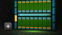
The architecture of the G300 is code-named Fermi and features about 3 billion transistors, 512 ALUs, up to 6 GiByte GDDR5 RAM and a 384-bit memory interface. Nvidia has not anything revealed about clock rates yet - therefore all details about capability are meant by clock which does not necessarily show the performance ratio of the final products to its predecessors.
With the Fermi architecture Nvidia more and more focuses on GPU computing and also uses those terms in their presentation. The former texture units turned into Load/Store units, the shader ALUs (which Nvidia formerly called stream processors) are Cuda core or Cuda processors now. Certainly chips basing on the Fermi architecture will be DirectX 11-compatible but Nvidia doesn't talk about that much.
Last edited:


")
