


SANDY BRIDGE
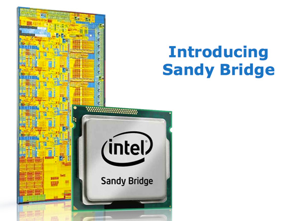
ඉන්ටෙල් සමාගම 2011 වෙළඳපොලට එවන අලුත්ම ප්රොසෙසර්(CPU) එක තමයි සැන්ඩි බ්රිජ්(Code Name - Sandy Bridge පස්සෙ නම වෙනස් වේවි). intel සමාගම කියන විදියට මේක මයික්රොචිප් වෙළඳපොල හොල්ලන්න පුලුවන් ප්රොසෙසර් එකක්. මොකද මේකෙ විශේෂ දෙයක් තමයි ග්රැෆික්ස් ප්රොසෙසර්(GPU) එකත් එකතු කරලම හදලා තියෙන්නේ(CPU+GPU=Combo Chip).
ඒ කියන්නේ වෙනම ග්රැෆික්ස් චිප් සෙට් එකක් නෑ.ප්රොසෙසර් එක ඇතුලෙම තමයි GPU එකත් තියෙන්නේ.
CPU හා GPU වෙන වෙනම තියනකොට ඒවා අතර සන්නිවේදනය කරන්න වෙන්නේ Motherboard එක හරහා නේ.එතකොට වැඩි කාලයක් වගේම වැඩි ශක්තියක් වැයවෙනවා. ඒත් මේ අලුත්ම ක්රමය නිසා ඒ දෙකම ඉතුරු වෙනවා වගේම performance වැඩි වෙනවා.
මේ චිප් එකේ තියන කෑෂ් මෙමරි එක(cache memory) මගින් 384GB/sec වේගයෙන් දත්ත හුවමාරු කරන්න ඇති හැකියාව නිසා දැනට තියන දත්ත හුවමාරු වේගය හතර ගුණයකින් වැඩි වෙන
බව කියවෙනවා.
2011 මුල් කාර්තුවේදි ඩෙස්ක්ටොප් හා ලැප්ටොප් දෙවර්ගයටම ප්රොසෙසර් නිකුත් කරන බවයි ඉන්ටෙල් කියන්නෙ.
තාම සම්පූර්ණ විස්තර හෙලිකරලා නෑ.දැනට හෙලිවෙලා තියන ටිකක් තමයි මේ.
# Standard CPU clock speed rated at 2.2 GHz to 3.4 GHz for variants. With Turbo Boost Technology enabled, up to 3.8 GHz clock speed can be achieved.
# Integrated graphics core running at 650 MHz to 850 MHz. With Turbo Boost Technology enabled, it can achieve up to 1350 MHz clock speed.
# Some amount of L3 cache will be disabled accordingly on some models in order to differentiate products among different market segments.
# 64 KB L1 cache/core (32 KB L1 Data + 32 KB L1 Instruction, 3 clocks) and 256 KB L2 cache/core (8 clocks).
# Up to 8 MB shared L3 cache (25 clocks) on a ring bus to be shared with the integrated graphics core.
# 256 bit/cycle Ring bus bandwidth. The ring bus connects the cores.
# All processors will feature a 64-byte cache line width.
# Decoded micro-op cache and enlarged, optimized branch predictor.
# Improved performance for transcendental math, AES encryption, and SHA-1 hashing.
# Thermal Design Power (TDP) of products are rated between 35...95 W for desktop variants, and 18...55 W for mobile variants.
# Dual-core and quad-core processors will be available at launch, with six-core and eight-core processors planned for future release.
# x86 peak performance (with and without AVX): 30.4 DP GFLOPS / 7.6 DP GFLOPS per core (8 DP FP / 2 DP FP Per clock) @ 3.8GHz
# Improved memory controller with maximum 25.6 GByte/s bandwidth supports DDR3-1600 dual channel RAM and two load/store operations per cycle.

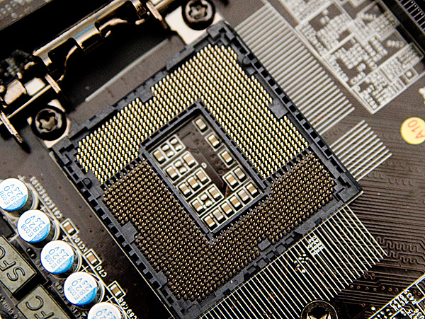
මේ තියෙන්නේ LGA1155 සොකට් එක.
අනිවාර්යෙන්ම මේක NVidia සහ ATI ග්රැෆික්ස් කාඩ් වෙළඳපොලට තර්ජනයක් වේවි. ඒ වගේම AMD සමාගමත් මේ තාක්ෂණය ගැන උනන්දුවෙන් ඉන්නවලු.
ඉන්ටෙල් සමාගම 2011 වෙළඳපොලට එවන අලුත්ම ප්රොසෙසර්(CPU) එක තමයි සැන්ඩි බ්රිජ්(Code Name - Sandy Bridge පස්සෙ නම වෙනස් වේවි). intel සමාගම කියන විදියට මේක මයික්රොචිප් වෙළඳපොල හොල්ලන්න පුලුවන් ප්රොසෙසර් එකක්. මොකද මේකෙ විශේෂ දෙයක් තමයි ග්රැෆික්ස් ප්රොසෙසර්(GPU) එකත් එකතු කරලම හදලා තියෙන්නේ(CPU+GPU=Combo Chip).
ඒ කියන්නේ වෙනම ග්රැෆික්ස් චිප් සෙට් එකක් නෑ.ප්රොසෙසර් එක ඇතුලෙම තමයි GPU එකත් තියෙන්නේ.
CPU හා GPU වෙන වෙනම තියනකොට ඒවා අතර සන්නිවේදනය කරන්න වෙන්නේ Motherboard එක හරහා නේ.එතකොට වැඩි කාලයක් වගේම වැඩි ශක්තියක් වැයවෙනවා. ඒත් මේ අලුත්ම ක්රමය නිසා ඒ දෙකම ඉතුරු වෙනවා වගේම performance වැඩි වෙනවා.
මේ චිප් එකේ තියන කෑෂ් මෙමරි එක(cache memory) මගින් 384GB/sec වේගයෙන් දත්ත හුවමාරු කරන්න ඇති හැකියාව නිසා දැනට තියන දත්ත හුවමාරු වේගය හතර ගුණයකින් වැඩි වෙන
බව කියවෙනවා.
2011 මුල් කාර්තුවේදි ඩෙස්ක්ටොප් හා ලැප්ටොප් දෙවර්ගයටම ප්රොසෙසර් නිකුත් කරන බවයි ඉන්ටෙල් කියන්නෙ.
තාම සම්පූර්ණ විස්තර හෙලිකරලා නෑ.දැනට හෙලිවෙලා තියන ටිකක් තමයි මේ.
# Standard CPU clock speed rated at 2.2 GHz to 3.4 GHz for variants. With Turbo Boost Technology enabled, up to 3.8 GHz clock speed can be achieved.
# Integrated graphics core running at 650 MHz to 850 MHz. With Turbo Boost Technology enabled, it can achieve up to 1350 MHz clock speed.
# Some amount of L3 cache will be disabled accordingly on some models in order to differentiate products among different market segments.
# 64 KB L1 cache/core (32 KB L1 Data + 32 KB L1 Instruction, 3 clocks) and 256 KB L2 cache/core (8 clocks).
# Up to 8 MB shared L3 cache (25 clocks) on a ring bus to be shared with the integrated graphics core.
# 256 bit/cycle Ring bus bandwidth. The ring bus connects the cores.
# All processors will feature a 64-byte cache line width.
# Decoded micro-op cache and enlarged, optimized branch predictor.
# Improved performance for transcendental math, AES encryption, and SHA-1 hashing.
# Thermal Design Power (TDP) of products are rated between 35...95 W for desktop variants, and 18...55 W for mobile variants.
# Dual-core and quad-core processors will be available at launch, with six-core and eight-core processors planned for future release.
# x86 peak performance (with and without AVX): 30.4 DP GFLOPS / 7.6 DP GFLOPS per core (8 DP FP / 2 DP FP Per clock) @ 3.8GHz
# Improved memory controller with maximum 25.6 GByte/s bandwidth supports DDR3-1600 dual channel RAM and two load/store operations per cycle.

මේ තියෙන්නේ LGA1155 සොකට් එක.
අනිවාර්යෙන්ම මේක NVidia සහ ATI ග්රැෆික්ස් කාඩ් වෙළඳපොලට තර්ජනයක් වේවි. ඒ වගේම AMD සමාගමත් මේ තාක්ෂණය ගැන උනන්දුවෙන් ඉන්නවලු.
Last edited:


