MOBILE PHONE REPAIRING GUIDE

laal

Member
Apr 18, 2008
185
9
0
Familarization: Components and Parts on Blackberry Mobile Phone Handsets

Here's a series of blackberry mobile phone products which is also one of the largest producers in mobile phone industry. Be familiar and remember each and every component parts how it differs from each other.

he BlackBerry Storm is the first touchscreen smartphone developed by Research In Motion. It is also the first device to implement physical feedback to a touchscreen device, labelled by RIM as "SurePress" technology.


http://draft.blogger.com/post-create.g?blogID=6231501182166011326
Product Features & Specifications

http://draft.blogger.com/post-create.g?blogID=6231501182166011326
Technical Specifications

Operating System BlackBerry OS 4.7 Network Support 9500: GSM/GPRS/EDGE/HSDPA, UMTS: 850/1900/2100MHz, GSM: 850/900/1800/1900MHz
9530: CDMA/1xRTT/EV-DO/Rev.A, CDMA: 800/1900MHz Screen 3.25" HVGA (360 x 480px), 65k Color TFT Input Method Glass Capacitive Touchscreen with SurePress technology Wi-Fi None GPS GPS and A-GPS Capable with integrated BB Maps Bluetooth Bluetooth v2.0, A2DP support Camera 3.2MP Camera with Auto Focus Storage Internal 1GB Storage, External MicroSDHC Slot Connection Ports 3.5mm stereo audio jack, Micro-USB 2.0 Physical Attributes Dimensions: 112.5mm x 62.2mm x 13.95mm, Weight: 155g http://draft.blogger.com/post-create.g?blogID=6231501182166011326
Media Support

Audio Support Codecs: MP3/WMA Pro Plus/AAC+/eAAC+ Video Support Codecs: MPEG4 H.263, H.264, WMV Browser BlackBerry Browser with Full HTML support and streaming video

http://draft.blogger.com/post-create.g?blogID=6231501182166011326
Bill of Materials

* represents unmarked ICs and best educated guesses
Processor Qualcomm MSM7600 Processor @ 624MHz Screen 3.25" HVGA LCD, 65k Color TFT Capacitive Sensor IC Synaptics* Storage Samsung MCP - 1GB MoviNAND, 1Gb OneNAND, 1Gb Mobile DDR USB PHY SMSC USB3316 Wi-Fi None Bluetooth CSR 63B23 GPS Integrated into Baseband Processor Audio Integrated into Baseband Processor Accelerometer STMicroelectronics* RF Transceiver Qualcomm RTR6500 CDMA/EV-DO, Qualcomm RTR6285 Multi-band UMTS/Quad-band GSM Power Management PMIC: Qualcomm PM7540
Power Amp (CDMA-850MHz): Avago ACPM-7813; Power Amp (CDMA-1900MHz): Avago ACPM-7833
Power Amp (Quad-band GSM): TriQuint Semiconductor 7M5012 http://draft.blogger.com/post-create.g?blogID=6231501182166011326
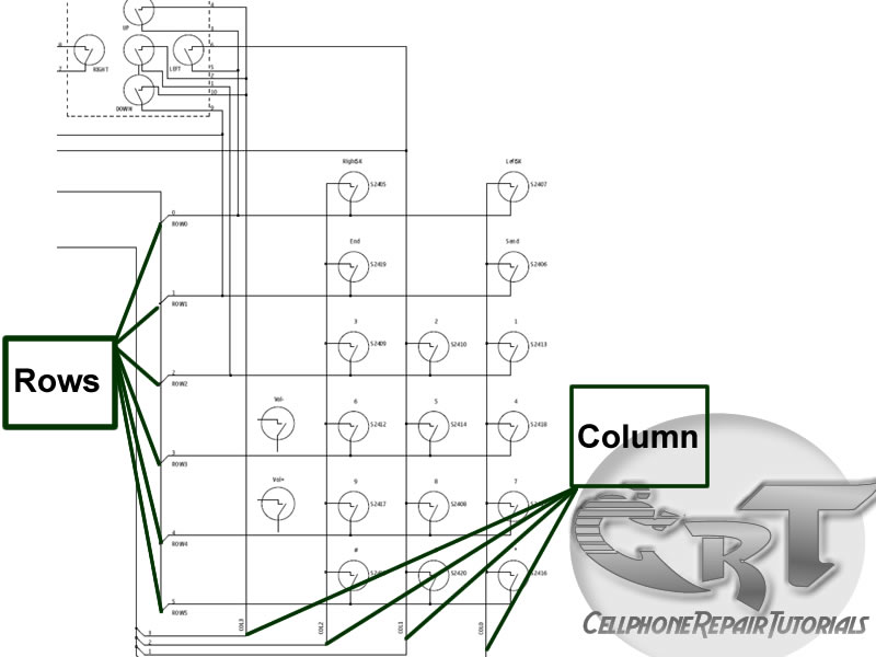
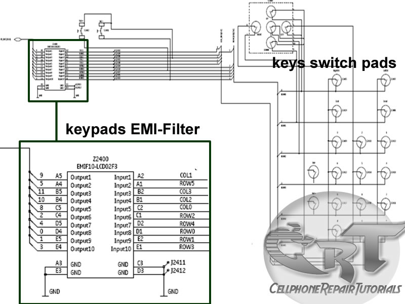
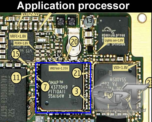
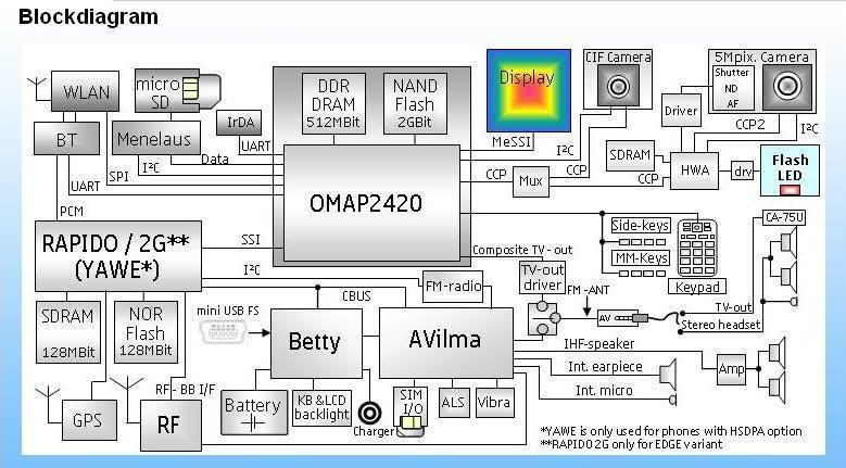
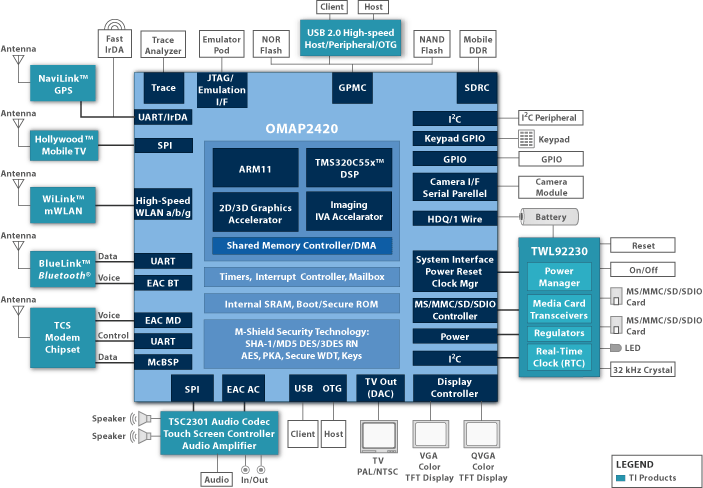
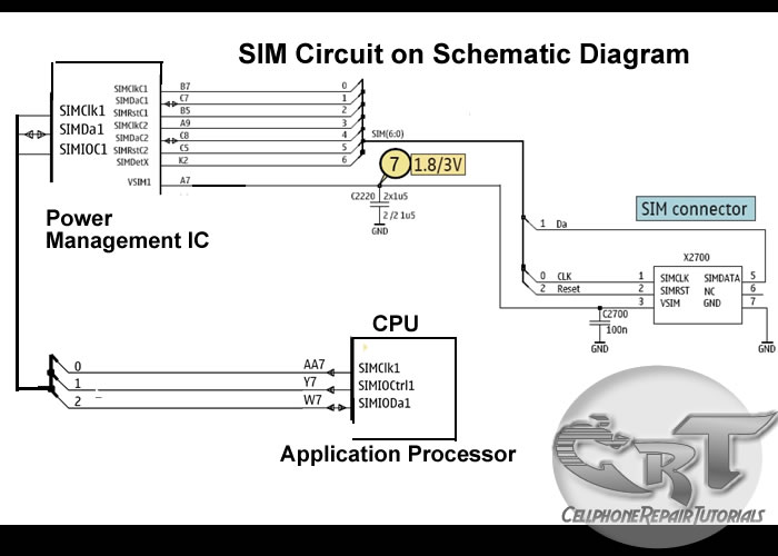
Block Diagram


http://draft.blogger.com/post-create.g?blogID=6231501182166011326
Teardown Pictures


The BlackBerry Bold is a smartphone developed by Research In Motion.


http://draft.blogger.com/post-create.g?blogID=6231501182166011326
Product Feature & Specifications

http://draft.blogger.com/post-create.g?blogID=6231501182166011326
Technical Specifications

Operating System BlackBerry OS 4.6 Network Support GSM/GPRS/EDGE/HSDPA, UMTS: 850/1900/2100MHz, GSM: 850/900/1800/1900MHz Screen 2.65" HVGA (320 x 480px), 65k Color TFT Input Method QWERTY Keyboard, Trackball Wi-Fi 802.11a/b/g GPS Internal GPS equipped with BB Maps Bluetooth Bluetooth v2.0, A2DP and AVCRP support Camera 2MP Camera with LED Flash Storage Internal 1GB Storage, External MicroSDHC Slot Connection Ports Mini-USB 2.0 Hi-Speed, 3.5mm stereo audio jack Physical Attributes Dimensions: 114mm x 66mm x 12.7mm, Weight: 133g http://draft.blogger.com/post-create.g?blogID=6231501182166011326
Media Support

Audio Support Codecs: MP3/WMA/AAC+ Video Support Codecs: DivX/XviD/WMV/3GP Browser Full HTML Browser, streaming video, RSS feed support

http://draft.blogger.com/post-create.g?blogID=6231501182166011326
Bill of Materials

Processor Marvell Tavor PXA930 @ 624Mhz Screen Samsung 2.65" HVGA LCD, 65k Color TFT Storage Samsung MCP - 1GB MoviNAND, 1Gb OneNAND, 1Gb Mobile DDR Wi-Fi Texas Instruments WL1253B GPS SiRF GSC3LTif USB 2.0 Mass Storage Cypress Semiconductor CYWB01294AB Audio Texas Instruments TLV320AIC3106IZQER RF Transceiver Infineon Tri-Band WCDMA/HSDPA, Renesas Quad-Band GSM/GPRS/EDGE Power Management PMIC: Texas Instruments TPS65850
Power Amp (GSM): Renesas
Power Amp (WCDMA-850/1900MHz): Anadigics; Power Amp (WCDMA-2100MHz): Anadigics
Power Amp (Wi-Fi 2.4GHz): Texas Instruments WL1251FE; Power Amp (Wi-Fi 5GHz): Texas Instruments WL1253FE

http://draft.blogger.com/post-create.g?blogID=6231501182166011326
Block Diagram


http://draft.blogger.com/post-create.g?blogID=6231501182166011326
Teardown Pictures


The BlackBerry Curve 8900 is a of smartphone developed by Research In Motion. It is the successor to the popular BlackBerry Curve 8300.


http://draft.blogger.com/post-edit.g?blogID=6231501182166011326&postID=3314555170161198565
Product Features & Specifications

http://draft.blogger.com/post-edit.g?blogID=6231501182166011326&postID=3314555170161198565
Technical Specifications

Operating System BlackBerry OS 4.6 Network Support GSM/GPRS/EDGE, GSM: 850/900/1800/1900MHz Screen 2.44" HVGA (320 x 480px), 65k Color TFT Input Method QWERTY Keyboard, Atomic Trackball Wi-Fi 802.11b/g with UMA support GPS Internal GPS equipped with BB Maps (On 8310) Bluetooth Bluetooth v2.0, A2DP and AVCRP support Camera 3.2MP Camera with LED Flash Storage Internal 256MB Storage, External MicroSDHC Slot Connection Ports Micro-USB 2.0 Hi-Speed, 3.5mm stereo audio jack Physical Attributes Dimension: 109mm x 60mm x 14mm, Weight: 112g http://draft.blogger.com/post-edit.g?blogID=6231501182166011326&postID=3314555170161198565
Media Support

Audio Support Codecs: MP3/WMA/AAC+ Video Support Codecs: DivX/WMV/XviD/3GP Browser BlackBerry Browser with full HTML support http://draft.blogger.com/post-edit.g?blogID=6231501182166011326&postID=3314555170161198565
Bill of Materials

Processor Freescale SC29746VK @ 512Mhz Processor Screen Samsung 2.44" HVGA LCD, 65k Color TFT Storage Samsung MCP - 1Gb OneNAND + Mobile DDR Wi-Fi Texas Instruments WL1253B GPS SiRF GSC3LTi USB 2.0 Mass Storage Cypress Semiconductor CYWB01294AB Audio Texas Instruments AC3106I (TLV320AIC3106I) RF Transceiver Freescale Quad-Band GSM/GPRS/EDGE Power Management PMIC: Texas Instruments TPS65851
Power Amp (GSM): Skyworks SKY77256-11
Power Amp (Wi-Fi 2.4GHz): Texas Instruments WL1251FE http://draft.blogger.com/post-edit.g?blogID=6231501182166011326&postID=3314555170161198565
Block Diagram


http://draft.blogger.com/post-edit.g?blogID=6231501182166011326&postID=3314555170161198565
Teardown Pictures


laal

Member
Apr 18, 2008
185
9
0
What is Power Mangement IC, How Does it supply power voltage to a Mobile Phones circu

Power Management IC is a power IC, that manage,control and distribute and Supply Power voltages from the battery source to other corresponding circuits or chips.
It is highly designed to convert,regulate, stabilize current and voltages that flow across unto it.
A power supply IC Chips can divide and multiply certain voltage from one desired voltage source to any desired power output voltages.
Which is for example a battery voltage source amounts at 3.7voltsDC while other components chips or circuit only requires the amount of 1.8volts, This 1.8volts is the amount of voltage is what the power management IC are going to convert.
A block diagram below shows a brief details on how power supply IC converts and distribute certain desired
voltage from a battery power source to other corresponding circuits or components.

In a typical schematic diagram like in Nokia mobile phones, certain output supply power voltages were labeled as how much the amount of each output to supply power voltages to another circuits or components.
A failure of a power management IC to gain this following output voltage is also a failure to other corresponding components or circuits to work.
A picture below is an example layout of a power management IC mounted on a printed circuit board.
A deep familiarization of how this chips works including its whole operation within a circuitry of mobile phones is also a powerful tool in troubleshooting hardware problem issues on a mobile phones.
 

laal

Member
Apr 18, 2008
185
9
0
What is An Application Processor in Mobile Phones Circuit Do

An application processor is a central proccessing unit (CPU) like the one installed on personal computer. It is the brain and controls all kind of data and information any application in mobile phones circuit.
It is microprocessor integrated circuit (IC) chip.


LCD controller, camera interface, serial interfaces, memory interface,USB controller, bluetooth and wifi controller,and more. are controlled by an the application processor.

Here's an example of an application processor block diagram below, on how this kind of IC works on mobile phones circuit. This kind of an application is commonly used on Nokia latest designed of mobile handsets. The description of this application processor below will help us understand how does this certain IC work.
l4_omap2420.gif


OMAP2420 Processor

The OMAP2420 processor is a single-chip applications processor that supports all cellular standards, and complements any modem or chipset and any air interface. It is intended for high-volume wireless handset manufacturers and is not available through distributors. The OMAP2420 includes the benefits of the OMAP 2 architecture’s parallel processing, giving users the ability to instantly run applications and operate multiple functions simultaneously without quality of service compromises. The OMAP2420 includes an integrated ARM1136 processor (330 MHz), a TI TMS320C55x™DSP (220 MHz), 2D/3D graphics accelerator, imaging and video accelerator, high-performance system interconnects and industry-standard peripherals.
Graphics

The OMAP2420 processor embeds Imagination Technologies' POWERVR MBX™ graphics core, making it the first applications processor to support OpenGL ES® 1.1 and OpenVG™, providing superior graphics performance and advanced user interface capabilities. TI is enabling sophisticated and dynamic images with "smart pixel" technology offered via OpenGL ES 1.1. This unique technology allows each pixel in an image to be programmed individually, giving developers the power to create rich effects with cinematic realism. Users will now experience "life-like" facial features, advanced reflection effects and multi-textured backgrounds in the mobile environment.

Multimedia enhancements made in the OMAP2420 include an added imaging and video accelerator for higher-resolution still capture applications, multi-megapixel cameras and full-motion video encode and decode with VGA resolution of 30 frames per second. An added TV video output supports connections to television displays for displaying images and video captured from the handset. 5-Mb internal SRAM also boost streaming media performance. Access to the OMAP Developer Network also provides an extensive range of programs and media components that manufacturers can use for differentiating and delivering products to market fast.
Key Features:


  • Dedicated 2D/3D graphics accelerator at 2 million polygons per second
  • Added imaging and video accelerator enables high-resolution still image capture, larger screen sizes and higher video frame rates
  • Supports high-end features including 4+ megapixel cameras, VGA-quality video, high-end interactive gaming functionality and analog/digital TV video output
  • 5-Mb internal SRAM boosts streaming media performance
  • Software compatibility with previous OMAP processors
  • Parallel processing ensures no interruptions or degradation of service with simultaneously running applications
  • Optimized power management companion chip, TWL92230 12 mm x 12 mm, 325-ball MicroStar BGA™, 0.5-mm pitch
 

laal

Member
Apr 18, 2008
185
9
0
What is NAND and NOR Flash Memories

There are two types of flash memory, NOR and NAND. The names refer to the type of logic gate used in each memory cell. (Logic gates are a fundamental building block of digital circuits). NOR flash memory was first introduced by Intel in 1988. NAND flash was introduced by Toshiba in 1989
The two chips work differently. NOR flash is faster, but it's also more expensive and takes longer to erase and write new data. NOR is most often used in mobile phones. NAND has significantly higher storage capacity than NOR. It has found a market in devices to which large files are frequently uploaded and replaced. MP3 players, digital cameras and USB drives use NAND flash.


NAND Flash is a special form of Flash memory. Flash memory is a memory technology that keeps data even when the power supply is cut off; this is known as a non-volatile memory type. Flash memory can be read pretty fast, but writing to Flash memory is pretty slow compared to many other -volatile- memory technologies such as SRAM or DRAM. Flash also has a limited number of write-cycles; manufacturers typically specify something in the area of 10,000 writes for the lifetime of the part.
NAND Flash is faster than regular Flash, although the general characteristics still hold.
Flash memory is widely used in digital cameras, portable MP3 players, USB (Flash) sticks, and many other devices.

NOR flash memory is a type of non-volatile storage technology that does not require power to retain data.
NAND devices are accessed serially, using the same eight pins to transmit control, addressing and data. NOR flash memory supports one-byte random access, which allows machine instructions to be retrieved and run directly from the chip, in the same way that a traditional computer will retrieve instructions directly from main memory. NOR flash has an SRAM interface that includes enough address pins to map the entire chip, enabling for access to every byte stored within it.

Some devices use both NAND and NOR. A pocket PC, for instance, may use embedded NOR to boot up the operating system and a removable NAND card for all its other memory or storage requirements.
 

laal

Member
Apr 18, 2008
185
9
0
What is RAM IC ? how does it work on mobile phones handsets

Random access memory (RAM) is used in mobile phones circuit to store memory datas. It is made of millions of transistors and capacitors that being packed into integrated circuit (IC)
Transistors and capacitors are paired to create a memory cell, which represent a single bit of data. The capacitor holds the bit data of information, a 0 or a 1. The transistor acts as a switch that lets the controlcircuitry on the memory chip read the capacitor or cahnge its state. In most cases common form of mobile phones memory is a Dynamic random access memory (DRAM)
The opposite of RAM is Serial Dynamic Random access memory (SAM). SAM stores data
as a series of memory cell that can only be access sequentially. If the data is not in the current location each memory cell is check until the needed data is found.


SDRAM
SDRAM stands for Synchronous Dynamic Random Access Memory. DDR is short for "DDR SDRAM" and stands for Double Data Rate. Nowadays to avoid misunderstandings SDRAM is often specified as SDR SDRAM and SDR stands for Single Data Rate by analogy with DDR. Therefore, the main difference between SDR and DDR memory the doubled speed: DDR can transfer data at roughly twice the speed of SDRAM.

DRAM. Dynamic Random Access Memory is used to temporarily store information on mobile phones. DRAM is made up of many cells and each cell is referred to as a bit. A cell contains a capacitor and a transistor. Since computer machine language is made up of 1s and 0s, it has the value of one when active and zero when inactive.
SDRAM or Synchronous Random Access Memory is the result of DRAM evolution. This type of memory synchronizes the input and output signals with the system board. Its speed ratings are in MHz. SDRAM was introduced in 1996 and is still used today. SDRAM transmits every clock count at a specific time.
DDR RAM (or Double Data Rate Random Access Memory) does the same but it does so twice every clock count. This makes DDR RAM twice as fast as SDRAM.
 

laal

Member
Apr 18, 2008
185
9
0
How does Charging Circuit Works from a Battery Charger to charge a Mobile phone Batte

This lesson is also important for charging problem troubleshooting for knowing which parts or components has being used to make a charging circuit. Many mobile phone technicians had been asking me, how does mobile phone charging circuit works? How does a battery charger can charge a mobile phone battery?
To tell the truth many of them has never heard of this even they already fix thousands of mobile phones in their years of cellphone repair careers." and I am one of them.
I don't know but I know how fix it, its so easy" that's what we've oftenly said.
Well, we all know that all mobile phones are all battery operated handsets that needs to charge the battery so that it will continue working, failure to charge it will result to unable to power up the mobile phone handsets.

Here's a brief explanation of how charging circuit works,
I prepare this simple idea and diminished some electronics technical terms so that everyone without adequate knowledge on electronics technical terms might can catch up with this.


A charging circuit is composed of the following stages or sections.

1. Battery Charger Circuits - Although this is not found on mobile phones PC board circuit and have separate circuit but definitely this is also part of charging circuit; without this, the charging circuit is not complete and will not work completely.
This circuit is all parts and components that being mounted on any mobile phone charger, this is the one that converts AC (Alternating Current)voltage to DC (Direct Current)voltage.
What is AC Voltage? This voltage is a power source that we used in our household appliances to work and operate, this voltage can cause risk of electric shock and very dangerous to humans when being touch.This kind of voltage has an alternate polarity.
What is DC voltage? This voltage is a low level voltage which typically found on any kind of batteries.
This kind of voltage have two polarities, the negative and the positive.

Here's how the battery charger works, the 110 or 220 AC volts coming from the electrical outlet at home or etc. will be converted to a desired DC voltage like 4.5 to 6 volt DC because the phone only accepts and can be operated into small amount of DC voltage.


A DC voltage output of a charger is only an artificial DC voltage, why is that? because only a battery cell can produce a 100% pure DC voltage.

2. Protection Circuit- this circuit is composed of a Fuse, Inductor coil Diode and Capacitors, before the DC voltage reach to the charging voltage control circuits the protection circuit is the one that control and check if that voltage is in exact amount. Let say the desired amount of DC voltage is only 5.6 volts above that point the fuse will be blown out to stop the voltage to flow so that it prevents damaging to another corresponding circuits.
In a protection circuit below of Nokia BB5 mobile phones a diode is the one that measure the amount of voltage from the battery charger, this diode has a reaching point of desired voltage to measure of how much amount of voltage will be allowed to flow within that line, when exceed to that desired point of voltage the diode will then cut it off.
like for example if that diode is being designed that only allows only 7 volts from the battery charger to flow on that line. Now, above that desired voltage let say that the voltage becomes 8 or higher the diode will then be reacts and destruct itself, this is what then so-called shorted component; so that the current will flow directly to ground and will not reach to the following or corresponding circuit. If the diode will cut off or shorted the fuse will tends to blow and totally cut the voltage line. The inductor coil's role is to filter unwanted voltage saturation, it rejects abnormal voltage modulation caused by electrostatic interference.

3. Charger Voltage Control Circuit - This is the stage where the charger voltage and current is being stabilized, amplified, rectified, regulated and other voltage purification process is being held in this area before it feeds to the battery. This kind of circuit commonly being pack in a chips together with another circuits.

A failure of this certain area will result on charging problem status. This area mostly called by most technician as a Charging IC it is because this circuit is inside in a particular IC chips, but eventually this circuit also accompanied by many other circuit types and not exclusive to a certain charging area.
This pictures shows is the next corresponding circuit from the protection circuit area. The voltage from charger is now then feeds into three terminal inputs of the charger voltage control circuits.
in this figure shows after the voltage stabilization and purification process the voltage is now then feeds to the battery terminal.

4. Charging Control Circuit - this is the area where the charging process is being monitored, this is the one that sends information to the application processor to start or stop the charging process. This area is part of Power management circuit, so-called POWER IC by many technicians.
In this picture that there are two terminal signal from the voltage control that sends data to the Charging control circuit, this two data signals will inform to the charging control circuit that a charger voltage is being entered or plug-in. After this charging control circuits receives the data it will then analyze and convert that data into digital signal then sends it to the Application processor.


The application processor which is the brain of all the circuits now then decide if all the data's are in correct or in right information to begin the process,
It always relies on the data that sends by the charging control circuit, then decide all data and completely process it.


Okay now lets take an example and apply this particular method on a mobile phone circuitry component layout, I have here a Nokia N95 board, which is a good way to start with, while we still working on advance training. Now, try to analyze and compare all of those previous picture above and combined them into each corresponding stages or section, in this manner you can build an step by step tracing procedure on how to deal charging problem issues.

In the picture above shows, how and where the voltage flow from a charger voltage source through the entire PC board circuit. This is the the method where you can start and manage how to locate and trace each and every component to find possible problems regarding charging problem issues.
 
  • Like
Reactions: wajiras

laal

Member
Apr 18, 2008
185
9
0
How to Repair Cellphone Not Charging, No Reponse, Charger Not Supported Problem Issue

There are few types of charging problem issues like Not Charging, No Charging Response and Charger Not Supported.
A problem issues with "Not Charging" shows on a display when a charger is being plug-in, this problem occurs when a required current or voltage is not enough to boost up and charge the mobile phones battery.
One reason of this problem is a faulty BSI Line, a BSI line is a Battery Size Indicator that tell the charging control circuit how's the batteries working status.


The battery has a BSI output indicator terminal that connected to its negatives terminal with desired value of resistor on it.

One other charging problem issues is the No charging response when a battery charger is being plug-in, it stays no response or nothing happens.
One reason of this is a faulty protection circuit section. this happens when there is no voltage reach to charging circuit indicators and controls. If the protection circuit breakdown this will result to "charging no response" situation. You need to check each components for short and open circuits. You may start from the fuse then to the coil and the diode.
Charger Not Supported problem is cause by a faulty BTEMP thermistor component, BTEMP stands for Battery Temperature, This is the one that monitors the battery temperature status during at charging status, if this one having a problem , it wont allow any charger to proceed to charging stage.
This all, is only a brief explanation of how charging problem issues occurs, while charging the mobile phones .
There are lots of ways on how to troubleshoot each and every kind of handsets. Hope at least, this one let help you understand how charging problem issues occurs, and by this you can gain ideas to move into a stage where you can practice how to troubleshoot this kind of issues.
 

laal

Member
Apr 18, 2008
185
9
0
How Do SIM Card Works on Mobile Phones Circuit

A SIM Card also known as Subscriber Identity Module, A SIM is a Smart Card that can store data from a cellular phone. Those data like identity, location and phone number, network authorization data, personal security keys, contact lists and stored text messages. Security features include authentication and encryption to protect data and prevent eavesdropping.

But how does this SIM card works within the mobile phones circuit? How does mobile phones reads and write data unto it?
In those particular questions above, If we learn answers unto it, we can solve problem issues regarding SIM related problems, like Insert Sim Card and etc.

Now here's a brief explanation on how does SIM Circuit Works on a mobile phones circuit.

A Sim Card have six pads that also corresponds to the six SIM connectors pins, but only five has totally have connection on the entire layout.
SIM DATA - this is a digital data that being stored on a SIM memory
SIM Clock - this is a clock frequency signal that being synchronize to the digital data to create data signal in order transfer or sends and receive data information.
SIM Reset - this is also a frequency signal that triggers or reset all synchronization process.
VSIM B+ Supply Voltage- This a power supply voltage used to activated the SIM circuit.
SIM Ground - a ground line voltage
The other one is not connected


A Typical block Diagram above shows on how SIM Circuit Works on a Cellular phones circuits.
In the layout the Sim Interface Connector connected directly to SIM Control Circuit. The SIM Control Circuit is the one the generates Clock frequency that triggers the SIM data storage, once the SIM is now being triggered, it is then now sends data information to the application processor to begin the process with. The application processor is the one that gathered all data information from the SIM memory, initiate and activate it, if all information is in desired status.
Those three particular lines of signal flows associated in the circuit shows how the synchronization is being applied. If one of those lines being cut off the sending and receiving process will breakdown, and will result to SIM problem issues. The Power Supply Voltage through the SIM is also remain stable otherwise a lack of voltage will not activate the SIM to work.


In a picture below an EMI-ESD Filter has been added to protect the circuit to an Electro-static Discharge and Electro-magnetic Interference disorders. This type of SIM connection circuit is an advantage to mobile phone technician for troubleshooting SIM related problem issues. Thus, type of particular EMI filter is very vulnerable and mostly create breakdown to the entire SIM connection.
The picture below is an equivalent layout of an EMI filter and its internal circuitry,
only both frequency and data lines is being filtered.
The EMI Filter is a tiny chips designed to protect SIM DATA, SIM Clock and SIM Reset data signals that flow across trough the SIM connector.
The EMI-ESD Filter is a highly integrated device designed to suppress EMI(Electromagnetic Interference) and RFI(Radio frequency Interference in a circuit. This filter includes ESD protection circuitry which prevents damaging the mobile phone application when subject to ESD ( ElectroStatic Discharge) surges up to 15 kV.

Here's an example of how the the SIM data signal flow across the printed circuit board.
Note: this is only shows where the signal flows from component to component connections.


A picture above is an alternative way by many mobile phone technician dealing with SIM problem issues on most Nokia Mobile Phones
 

laal

Member
Apr 18, 2008
185
9
0
How Do SIM Card Works on Mobile Phones Circuit

A SIM Card also known as Subscriber Identity Module, A SIM is a Smart Card that can store data from a cellular phone. Those data like identity, location and phone number, network authorization data, personal security keys, contact lists and stored text messages. Security features include authentication and encryption to protect data and prevent eavesdropping.

But how does this SIM card works within the mobile phones circuit? How does mobile phones reads and write data unto it?
In those particular questions above, If we learn answers unto it, we can solve problem issues regarding SIM related problems, like Insert Sim Card and etc.

Now here's a brief explanation on how does SIM Circuit Works on a mobile phones circuit.

A Sim Card have six pads that also corresponds to the six SIM connectors pins, but only five has totally have connection on the entire layout.
SIM DATA - this is a digital data that being stored on a SIM memory
SIM Clock - this is a clock frequency signal that being synchronize to the digital data to create data signal in order transfer or sends and receive data information.
SIM Reset - this is also a frequency signal that triggers or reset all synchronization process.
VSIM B+ Supply Voltage- This a power supply voltage used to activated the SIM circuit.
SIM Ground - a ground line voltage
The other one is not connected


A Typical block Diagram above shows on how SIM Circuit Works on a Cellular phones circuits.
In the layout the Sim Interface Connector connected directly to SIM Control Circuit. The SIM Control Circuit is the one the generates Clock frequency that triggers the SIM data storage, once the SIM is now being triggered, it is then now sends data information to the application processor to begin the process with. The application processor is the one that gathered all data information from the SIM memory, initiate and activate it, if all information is in desired status.
Those three particular lines of signal flows associated in the circuit shows how the synchronization is being applied. If one of those lines being cut off the sending and receiving process will breakdown, and will result to SIM problem issues. The Power Supply Voltage through the SIM is also remain stable otherwise a lack of voltage will not activate the SIM to work.


In a picture below an EMI-ESD Filter has been added to protect the circuit to an Electro-static Discharge and Electro-magnetic Interference disorders. This type of SIM connection circuit is an advantage to mobile phone technician for troubleshooting SIM related problem issues. Thus, type of particular EMI filter is very vulnerable and mostly create breakdown to the entire SIM connection.
The picture below is an equivalent layout of an EMI filter and its internal circuitry,
only both frequency and data lines is being filtered.
The EMI Filter is a tiny chips designed to protect SIM DATA, SIM Clock and SIM Reset data signals that flow across trough the SIM connector.
The EMI-ESD Filter is a highly integrated device designed to suppress EMI(Electromagnetic Interference) and RFI(Radio frequency Interference in a circuit. This filter includes ESD protection circuitry which prevents damaging the mobile phone application when subject to ESD ( ElectroStatic Discharge) surges up to 15 kV.

Here's an example of how the the SIM data signal flow across the printed circuit board.
Note: this is only shows where the signal flows from component to component connections.


A picture above is an alternative way by many mobile phone technician dealing with SIM problem issues on most Nokia Mobile Phones.
 

laal

Member
Apr 18, 2008
185
9
0
Understanding Keypads Circuit, a way to Learn How to Repair Keypad Problem

Understanding the Keypad circuit may help and boost your knowledge on fixing keypad problem issues on mobile phones. Keypads is a part of user interface being used to navigate or enter numbers, letters and characters, browse application, sends information and etc.

An schematic diagram below will help us understand how keypad circuits works and which components or parts did this circuit is being connected.
In this diagram the each and every key switching pads is being divided and grouped into rows and columns. Each rows and columns were group into 2 -5 keypads switch. This rows and columns have each corresponding lines according to each and every group of switching pads.


This lines of rows and columns is being filtered for EMI and ESD protection the EMI filter is made of tiny chip that used to protect such EMI and ESD interference.
This rows and columns lines are digital switching signals generated by the application processor to trigger or activate every corresponding digital datas that is being stored and programmed within the mobile phone system memory. This diagram below is an Application Processor that generates and feeds then receives digital data switching signals.
This digital data frequency signals corresponds and interpreted to each key characters that are marked on each keypads. Like for example a combination of row 2 and column 3 will triggered the number 3 when hitting on it.
this block diagram below shows how the switching signal is being triggered to process a command data.
Various mobile phones have different keypads layouts and specification. A joystick and a volume switch is also parts of keypads switching circuits. Some keypads module designs are made into a flexible wire like those Slide Type package of mobile phones. Some flexible wires are very vulnerable and common cause of keypad malfunction.
 

laal

Member
Apr 18, 2008
185
9
0
How to Map and Trace keypads Lines

There are few methods in tracing and mapping the keypad layout on a mobile phones keypads on printed circuit board. One of this quick and very easy method is by using an schematic diagram, if that certain mobile phones have available unto it. Schematic diagram is very useful guide in every aspects of hardware troubleshooting.

Now assuming that you already have knowledge how to use and read it, follow this simple steps below.
Browse to bottom of the pages where yo can locate and find like the picture below., it is the keypad circuit section. In that schematic layout you will notice that each corresponding key characters is being group into lines. This group of keypad switch lines is being marked with rows and columns.


trace each and every lines where those keypads switch symbols is being connected, once you been manage to trace it. configure and trace it on the printed circuit board by using an analog or digital multimeter, just set it the resistance value X1 and attach both probes to corresponding keypads groups in every rows and column

Practice this kind of method with an aide of schematic diagram, in this way if you're skills grows further, you can then trace any other mobile phones without any schematic diagram available at first hand.
 

laal

Member
Apr 18, 2008
185
9
0
How Do LED light bulbs works on Mobile Phone Circuit

An LED - light emitting diode is used to illuminate keypads keys and LCD screen displays on all mobile phones handsets. It is being controlled by a voltage or current draws on its terminal leds.
a picture below is an Schematic Diagram that tells us how does the LED circuit works on cellular phone whole circuitry.

On schematic diagram we notice that the LEDs is driven by an LED driver chip's, and an Switching Control circuit that also being packed in a chip. The LED driver is being used to stabilized the voltage and current and do take control on engaging ON and OFF status of an LEDs to light up or not.
It also drives the amount of brightness or dimming status of the LEDs by applying Pulse Width Modulation signal from the Switching control circuit.

The block diagram below interpreted a component and section or parts of an LED circuit to work during application process.
The Switching control circuit feeds and release a Pulse Width Modulation Signal (PWM) to switch and light up the LEDs light bulbs. A pulse width modulation signal is a type of digital frequency signal range up to 1khz to enable and implement to take control of LED brightness.
Once that certain signal is being received by the LED driver, the LED driver now will engage and release the voltage or current that being feeds up from the mobile phones battery supply voltage;
The output voltage release by the LED driver is the one that draws the LED light bulbs to light up.


LED drivers is a high frequency, synchronous boost converter with constant current output to drive up to 5 white LEDs. This device circuit is designed for maximum safety, it integrates overvoltage and short circuit protection when the output is being shorted to the ground. Meaning this chips circuitry will not easily breakdown for it is designed to protect when short circuit happens.
like for example, the two LED light bulbs commits short circuit to its terminal
In mobile phones application methods; the switching control circuit that release pulse switching signal is also being synchronized programmed by the the application processor (CPU) to engaged a full control on how and which proper situation that the LED will be switch to light up or not.
like for example the LED will only switch and light up, if the handset is being in used and remain off if the handset is not in used.
The above image is an example of the LED circuit, how those particular stages and components being mounted on a phones circuits. Note that the LED driver and switching control circuits is being packed into an Integrated Circuit or ICs.


To all beginners: A bunch of simplified STEP By STEP Procedures On Troubleshooting LED Problem issues on various mobile phones product will be Posted Here Later.. Just keep on visiting this blog more often.
 

laal

Member
Apr 18, 2008
185
9
0
The Audio Codec is a circuit that controls sound signals in a cellphone circuits. It acts like an audio amplifier or an audio mixer or a sound booster.
Audio codec is the main area in a mobile phone where all audio properties is being process, during transmission and receiption. It converts the sound signal into radio frequency signal, and also converts radio frequency signal into a sound signals.
Like for example a microphone's sound signal is being amplified then converts and feeds to radio frequency before it send to the network airwaves. Opposite to that process is the conversion of radio frequency into an audible or understandable sound, and that sound is that what we hear on the earpiece speaker.
A typical block diagram below show how audio interfaces being connected to an audio codec circuit.

The Audio codec is the main part which control all audio properties from all audio interfaces like the microphone, earpiece, IHF (integrated hands free) speaker or a buzzer, ringer, head set and vibrator motor. A typical audio circuit is being filtered from any sound interference signal to avoid sound interruptions.